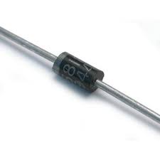
5W ZENER DIODE - ON This is a complete series of 5 Watt Zener diodes with tight limits and better operating characteristics that reflect the superior capabilities of silicon−oxide passivated junctions. All this in an axial lead, transfer−molded plastic package that offers protection in all common environmental conditions. Features • Zener Voltage Range − 3.3 V to 200 V • ESD Rating of Class 3 (& gt;16 kV) per Human Body Model • Surge Rating of up to 180 W @ 8.3 ms • Maximum Limits Guaranteed on up to Six Electrical Parameters • Pb−Free Packages are Available* Mechanical Characteristics CASE: Void free, transfer−molded, thermosetting plastic FINISH: All external surfaces are corrosion resistant and leads are readily solderable MAXIMUM LEAD TEMPERATURE FOR SOLDERING PURPOSES: 260°C, 1/16 in. from the case for 10 seconds POLARITY: Cathode indicated by polarity band MOUNTING POSITION: Any 1. Max operating temperature for DC conditions is 150°C, but not to exceed 200°C for pulsed conditions with low duty cycle or non−repetitive. 2. TOLERANCE AND TYPE NUMBER DESIGNATION: The JEDEC type numbers shown indicate a tolerance of ±5%. 3. ZENER VOLTAGE (VZ) and IMPEDANCE (IZT and IZK): Test conditions for zener voltage and impedance are as follows: IZ is applied 40 ±10 ms prior to reading. Mounting contacts are located 3/8″ to 1/2″ from the inside edge of mounting clips to the body of the diode (TA = 25°C +8°C, −2°C). 4. SURGE CURRENT (IR): Surge current is specified as the maximum allowable peak, non−recurrent square−wave current with a pulse width, PW, of 8.3 ms. The data given in Figure 5 may be used to find the maximum surge current for a square wave of any pulse width between 1 ms and 1000 ms by plotting the applicable points on logarithmic paper. Examples of this, using the 3.3 V and 200 V zener are shown in Figure 6. Mounting contact located as specified in Note 2 (TA = 25°C +8°C, −2°C). 5. VOLTAGE REGULATION (VZ): The conditions for voltage regulation are as follows: VZ measurements are made at 10% and then at 50% of the IZ max value listed in the electrical characteristics table. The test current time duration for each VZ measurement is 40 ±10 ms. Mounting contact located as specified in Note 2 (TA = 25°C +8°C, −2°C). 6. MAXIMUM REGULATOR CURRENT (IZM): The maximum current shown is based on the maximum voltage of a 5% type unit, therefore, it applies only to the B−suffix device. The actual IZM for any device may not exceed the value of 5 watts divided by the actual VZ of the device. TL = 25°C at 3/8″ maximum from the device body. 7. TOLERANCE AND TYPE NUMBER DESIGNATION: The JEDEC type numbers shown indicate a tolerance of ±5%. 8. ZENER VOLTAGE (VZ) and IMPEDANCE (IZT and IZK): Test conditions for zener voltage and impedance are as follows: IZ is applied 40 ±10 ms prior to reading. Mounting contacts are located 3/8″ to 1/2″ from the inside edge of mounting clips to the body of the diode (TA = 25°C +8°C, −2°C). 9. SURGE CURRENT (IR): Surge current is specified as the maximum allowable peak, non−recurrent square−wave current with a pulse width, PW, of 8.3 ms. The data given in Figure 5 may be used to find the maximum surge current for a square wave of any pulse width between 1 ms and 1000 ms by plotting the applicable points on logarithmic paper. Examples of this, using the 3.3 V and 200 V zener are shown in Figure 6. Mounting contact located as specified in Note 7 (TA = 25°C +8°C, −2°C). 10.VOLTAGE REGULATION (VZ): The conditions for voltage regulation are as follows: VZ measurements are made at 10% and then at 50% of the IZ max value listed in the electrical characteristics table. The test current time duration for each VZ measurement is 40 ±10 ms. Mounting contact located as specified in Note 7 (TA = 25°C +8°C, −2°C). 11. MAXIMUM REGULATOR CURRENT (IZM): The maximum current shown is based on the maximum voltage of a 5% type unit, therefore, it applies only to the B−suffix device. The actual IZM for any device may not exceed the value of 5 watts divided by the actual VZ of the device. TL = 25°C at 3/8″ maximum from the device body. FULL SERIES AVAILABLE AT BEST PRICE, SURAJ ELECTRONICS, MUMBAI.

This is your website preview.
Currently it only shows your basic business info. Start adding relevant business details such as description, images and products or services to gain your customers attention by using Boost 360 android app / iOS App / web portal.
5W ZENER DIODE - ON This is a complete series of ...
2021-10-28T07:18:11
5W ZENER DIODE - ON This is a complete series of 5 Watt Zener diodes with tight limits and better operating characteristics that reflect the superior capabilities of silicon−oxide passivated junctions. All this in an axial lead, transfer−molded plastic package that offers protection in all common environmental conditions. Features • Zener Voltage Range − 3.3 V to 200 V • ESD Rating of Class 3 (& gt;16 kV) per Human Body Model • Surge Rating of up to 180 W @ 8.3 ms • Maximum Limits Guaranteed on up to Six Electrical Parameters • Pb−Free Packages are Available* Mechanical Characteristics CASE: Void free, transfer−molded, thermosetting plastic FINISH: All external surfaces are corrosion resistant and leads are readily solderable MAXIMUM LEAD TEMPERATURE FOR SOLDERING PURPOSES: 260°C, 1/16 in. from the case for 10 seconds POLARITY: Cathode indicated by polarity band MOUNTING POSITION: Any 1. Max operating temperature for DC conditions is 150°C, but not to exceed 200°C for pulsed conditions with low duty cycle or non−repetitive. 2. TOLERANCE AND TYPE NUMBER DESIGNATION: The JEDEC type numbers shown indicate a tolerance of ±5%. 3. ZENER VOLTAGE (VZ) and IMPEDANCE (IZT and IZK): Test conditions for zener voltage and impedance are as follows: IZ is applied 40 ±10 ms prior to reading. Mounting contacts are located 3/8″ to 1/2″ from the inside edge of mounting clips to the body of the diode (TA = 25°C +8°C, −2°C). 4. SURGE CURRENT (IR): Surge current is specified as the maximum allowable peak, non−recurrent square−wave current with a pulse width, PW, of 8.3 ms. The data given in Figure 5 may be used to find the maximum surge current for a square wave of any pulse width between 1 ms and 1000 ms by plotting the applicable points on logarithmic paper. Examples of this, using the 3.3 V and 200 V zener are shown in Figure 6. Mounting contact located as specified in Note 2 (TA = 25°C +8°C, −2°C). 5. VOLTAGE REGULATION (VZ): The conditions for voltage regulation are as follows: VZ measurements are made at 10% and then at 50% of the IZ max value listed in the electrical characteristics table. The test current time duration for each VZ measurement is 40 ±10 ms. Mounting contact located as specified in Note 2 (TA = 25°C +8°C, −2°C). 6. MAXIMUM REGULATOR CURRENT (IZM): The maximum current shown is based on the maximum voltage of a 5% type unit, therefore, it applies only to the B−suffix device. The actual IZM for any device may not exceed the value of 5 watts divided by the actual VZ of the device. TL = 25°C at 3/8″ maximum from the device body. 7. TOLERANCE AND TYPE NUMBER DESIGNATION: The JEDEC type numbers shown indicate a tolerance of ±5%. 8. ZENER VOLTAGE (VZ) and IMPEDANCE (IZT and IZK): Test conditions for zener voltage and impedance are as follows: IZ is applied 40 ±10 ms prior to reading. Mounting contacts are located 3/8″ to 1/2″ from the inside edge of mounting clips to the body of the diode (TA = 25°C +8°C, −2°C). 9. SURGE CURRENT (IR): Surge current is specified as the maximum allowable peak, non−recurrent square−wave current with a pulse width, PW, of 8.3 ms. The data given in Figure 5 may be used to find the maximum surge current for a square wave of any pulse width between 1 ms and 1000 ms by plotting the applicable points on logarithmic paper. Examples of this, using the 3.3 V and 200 V zener are shown in Figure 6. Mounting contact located as specified in Note 7 (TA = 25°C +8°C, −2°C). 10.VOLTAGE REGULATION (VZ): The conditions for voltage regulation are as follows: VZ measurements are made at 10% and then at 50% of the IZ max value listed in the electrical characteristics table. The test current time duration for each VZ measurement is 40 ±10 ms. Mounting contact located as specified in Note 7 (TA = 25°C +8°C, −2°C). 11. MAXIMUM REGULATOR CURRENT (IZM): The maximum current shown is based on the maximum voltage of a 5% type unit, therefore, it applies only to the B−suffix device. The actual IZM for any device may not exceed the value of 5 watts divided by the actual VZ of the device. TL = 25°C at 3/8″ maximum from the device body. FULL SERIES AVAILABLE AT BEST PRICE, SURAJ ELECTRONICS, MUMBAI.
2021-10-28T07:18:11
Share it on


Keywords
- ±
- 6.
- 5.
- kV
- PW
- 9.
- TL
- 11.
- The
- IZT
- IZK
- 150
- 25°C
- 1 ms
- data
- CASE
- Note
- leads
- 200°C
- 3.3 V
- Class
- 180 W
- MUMBAI
- FINISH
- common
- Figure
- 8.3 ms
- reading
- Cathode
- 1000 ms
- 5 watts
- Examples
- Features
- IMPEDANCE
- TOLERANCE
- corrosion
- actual VZ
- actual IZM
- ESD Rating
- protection
- axial lead
- 10 seconds
- BEST PRICE
- device body
- 200 V zener
- FULL SERIES
- pulse width
- square wave
- inside edge
- Surge Rating
- 5% type unit
- tight limits
- IZ max value
- 3/8″ maximum
- polarity band
- DC conditions
- 5W ZENER DIODE
- Maximum Limits
- mounting clips
- low duty cycle
- maximum current
- maximum voltage
- B−suffix device
- Test conditions
- VZ measurements
- complete series
- Mounting contact
- Pb−Free Packages
- Human Body Model
- Mounting contacts
- MOUNTING POSITION
- SURAJ ELECTRONICS
- logarithmic paper
- applicable points
- external surfaces
- MAXIMUM REGULATOR
- pulsed conditions
- VOLTAGE REGULATION
- SOLDERING PURPOSES
- JEDEC type numbers
- 5 Watt Zener diodes
- Zener Voltage Range
- maximum surge current
- superior capabilities
- maximum allowable peak
- TYPE NUMBER DESIGNATION
- environmental conditions
- MAXIMUM LEAD TEMPERATURE
- Max operating temperature
- operating characteristics
- Six Electrical Parameters
- Mechanical Characteristics
- test current time duration
- transfer−molded plastic package
- electrical characteristics table
- non−recurrent square−wave current
- silicon−oxide passivated junctions
Submit Your Enquiry